Hardware assembly
Dec 22, 2014
Assemble the REV_B board and errata
After a while the REV_B PCBs arrived. So I instantly started to assemble the board. I will give you some insight in the process of the Surface Mount Technology (SMT) and tools I use. Then there where some pitfalls and workarounds I will show.
Shrinking the board
Remember, that I am still quite new to the surface mount devices. From REV_A to REV_B I changed all passive components from the 1206 to the 0603 package format. There are imperial (inch) and metric (mm) size form factors. Unfortunately the 0603 exists in both. In inch it is 1.6mm long and 0.8mm wide. After some practice, I could handle this size, although the 1206 inch size with its length of 3.2mm and width of 1.6mm is a bit easier to handle. By mistake I ordered a few hundred metric 0603 (an imperial 0201) capacitors. These are 0.6mm long and 0.3 mm wide. I guess it is nearly impossible to solder them reliable using a solder iron. Find a overview on the sizes here.
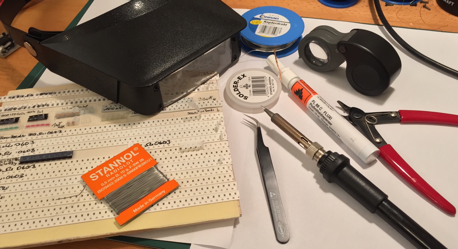
The tooling
I wanted to shrink the board and still use small and simple tools for the assembly. I don’t have the room for a reflow oven and all that stuff.
Here is my basic toolset:
- Good SMT tweezers (look for anti-magnetic, anti-static good quality)
- Soldering iron with 0.8mm flat tip (I use a analog regulated 80W station)
- Solder wick 1mm width
- Leaded solder in 0.5mm diameter
- Flux pen dispenser
- Magnifying lens 15x
- Clockmaker magnifying lens cap
- 0.4 mm tinned copper wire (mainly for the vias)
- Wire cutter (not used for SMT)
- Ohmmeter with connection tester
I wear the clockmaker magnifying lens with low magnification, because for soldering I don’t need to see all the details. I flux the pads and tin one pad. The pad doesn’t need to be completely covered. Then I hold the SMD component with the tweezers and touch the component pin and pad with the solder tip by putting the flat part on the pad. Because of the small component and pad it takes only one to two seconds to see the solder flow. I use 320 to 400°C for soldering. If one pad is a ground pad with a some connections to larger PCB areas it may take a little longer to solder. Take your time, I didn’t burn a part up to now.
Larger components like the XMEGA can be soldered the same way. Fix one pin, then another one on the oposite edge. After that the pins can be soldered one by one.
Then I use the 15x magnifying lens with some light (holding the PCB against a lamp can help as long as there are no big components mounted) to check for good solder and no unwanted shortcuts. If there is a shortcut, don’t panic. Flux the area, put a fresh end of the solder wick on the tinned part and the solder iron tip on top. The wick will soak up the solder.
An Ohmmeter with a connection tester is a good companion. My multimeter has a mode, in which it will beep, if there is a connection. So I don’t need to look up to see if there is a wanted or unwanted connection. Test for the wanted connections and unwanted ones.
After soldering the board I needed some time to find out unwanted connections like Ground to Vcc and many more.
A great tip I found very useful is to fix the SMD belts on a small board using double sided duct tape. I wrote the values on the stripes. So everything is sorted and fixed.
Assembly time!
I ordered the board etched, tinned and drilled. So there are no connected vias and no solder or print masks. So first I removed all layers expect the routes, vias and components with their names in Eagle PCB to create a plan for assembling. You will find these assembly plans in the Github repository in the hardware REV_B folder. I printed these in A4 and marked the parts values by hand on it.
The drill mask for the Allegro hall sensor big pins is incomplete. So I used a drill to create the long holes needed. To connect the vias, I laid the board on a flat surface, put 0.4mm tinned copper wire trough the holes and cut 2mm above. After 4 - 8 vias, I apply flux and solder them. After all the other side can be soldered and the exzessive wire cut away.
Then I soldered the components on the top side (the µC side). I started with the small components inside out. Be aware, that diodes are polarized and get the direction right. The have a point or stripe on the minus pin. See the result on the next picture:
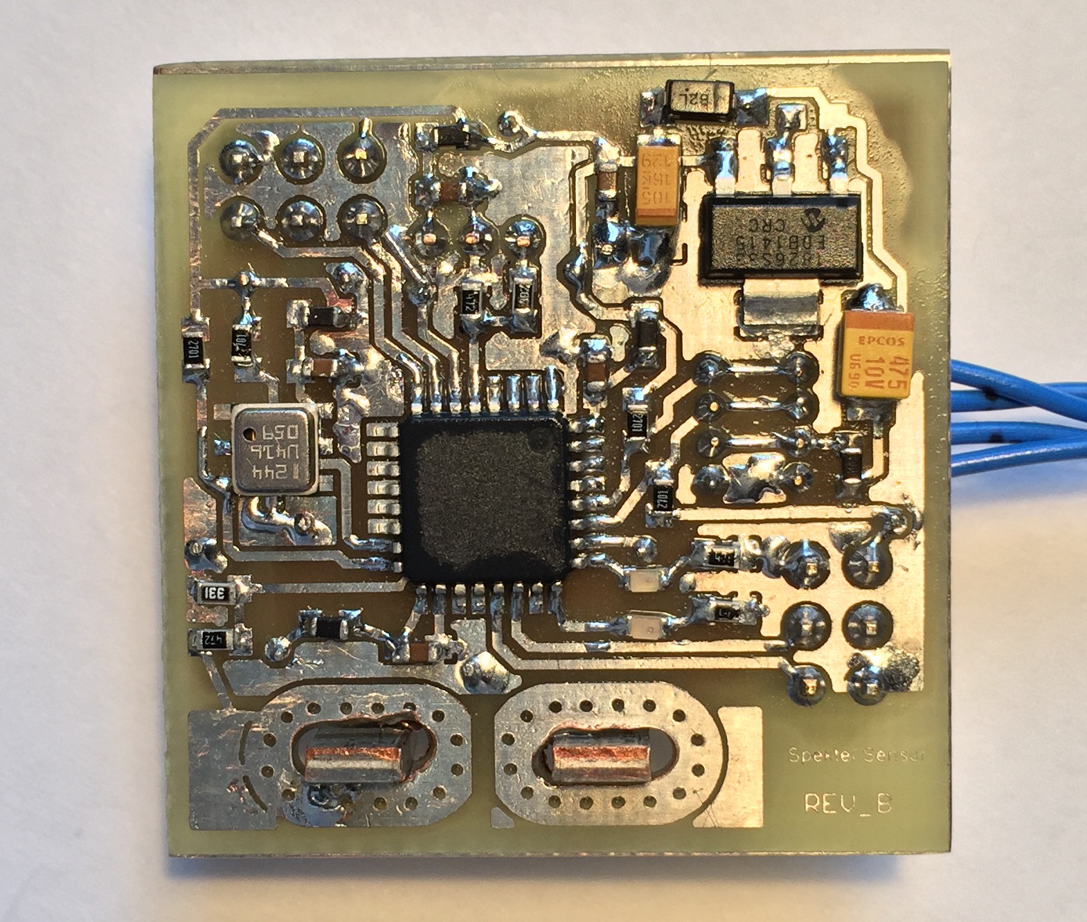
The Allegro current pins are not soldered yet.
In the B revision I tried to avoid using pins as vias, since it is difficult to solder a pin header from its top. But it is necessary in two cases as shown in the errata later on. The bottom side is much easier, because the two pin headers, two X-Bus connectors, the Allegro sensor and button take almost all of the space.
Assembling the BMP180
The self created footprint of the BMP180 in Eagle is a little bit larger, so that there is enough place for the soldering tip. Put solder on the connected pads. Be careful to get the pads filled, but don’t spend to much solder. Then flux, position the sensor - the pads are on the very edges - and heat while supplying little pressure with the tweezers. The BMP180 should level 100% with the board. Look from the side to see if it’s completely flat on the board with no gap or seam. The metal case of the sensor must have a connection to ground.
Errata
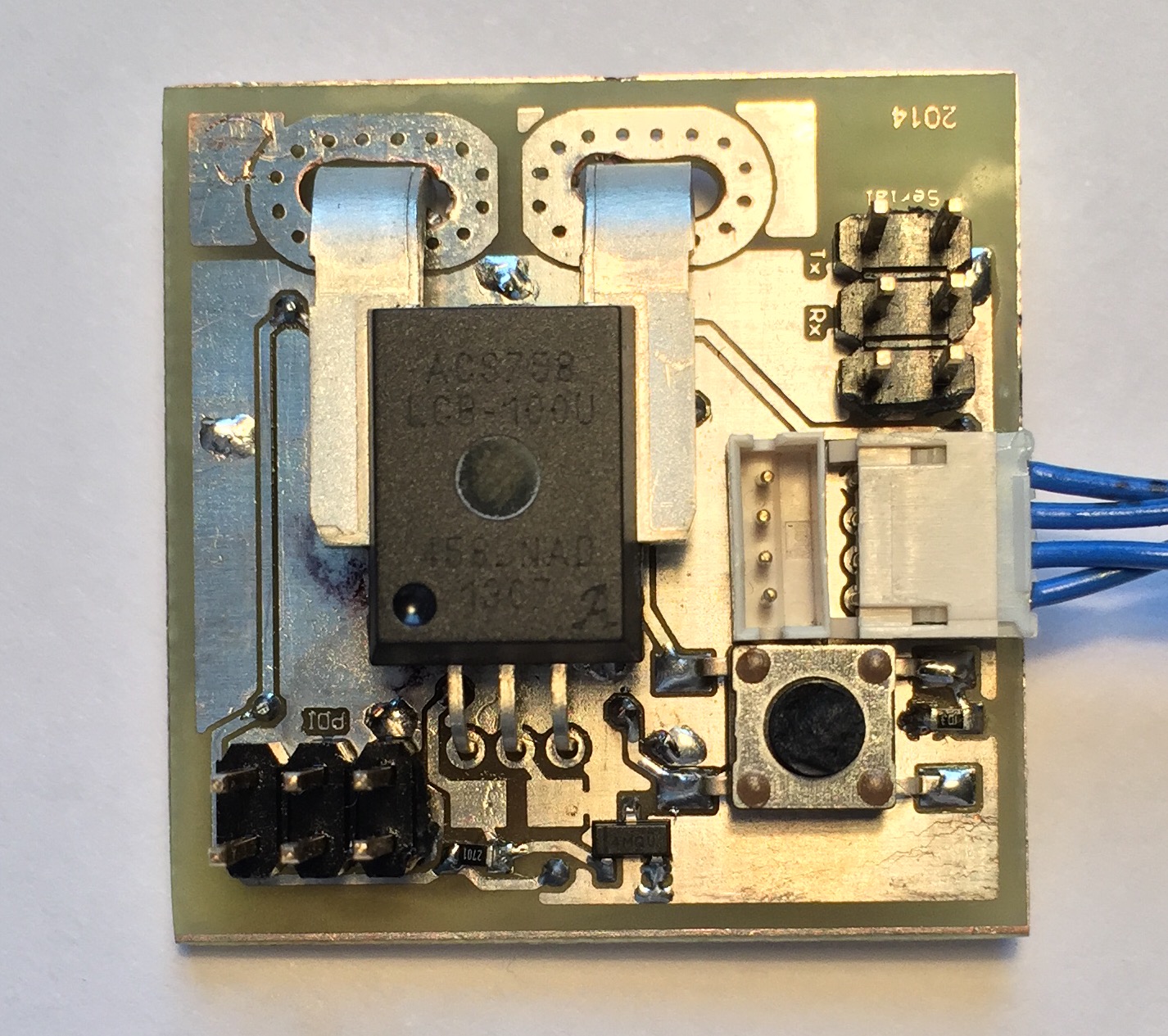
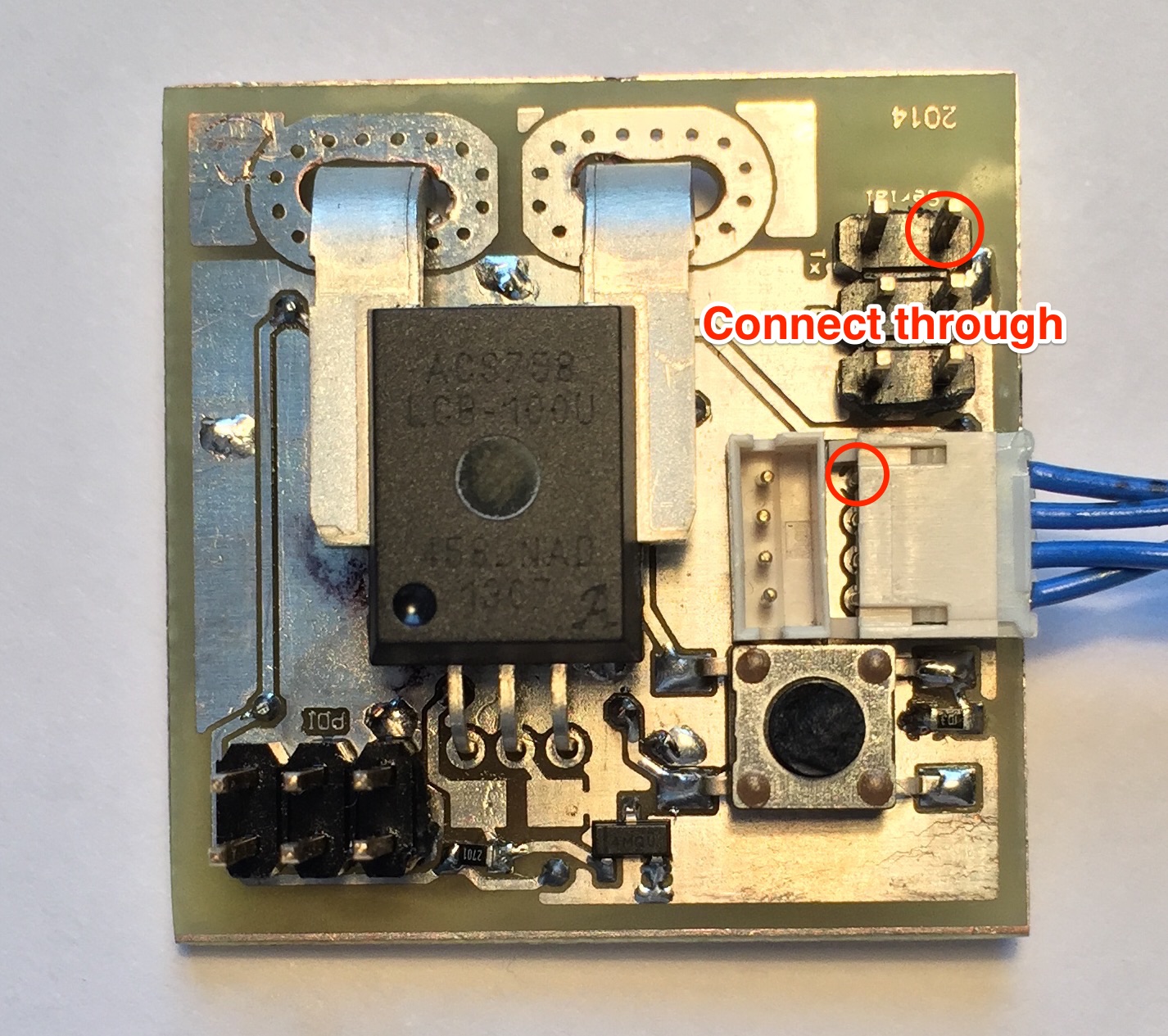
Again, there are some small faults on the board. Or at least things to optimize. I put the connectors on the bottom side, so that most of the soldering can be made on the top side only. The ground pin of the X-Bus ZH connectors needs to be connected to the bottom side. At least the angled connector can be soldered more easy than the straight one. Make sure to solder this before assembling the straight connector. If you only use this sensor, only one connector is needed anyway.
Second, the ground pin of the Serial connector needs to be connected to the bottom plate. I used an exacto knife to remove the plastic around the pin. With lots of flux the pin then can be soldered.
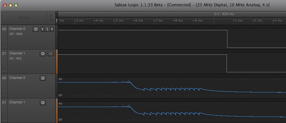
The I2C / TWI bus used to connect the Bosch BMP180 pressure sensor has two pull-up resistors. I tried to be smarter than the datasheet and put 2.7K in. It turned out, that they are two small to drive the SDA and SCL lines to GND fast enough. So use 4.7K for R4 and R5 instead.
I got myself a Saleae Logic8 logic analyser. Why it is probably not the most needed tool, in this case it helps a lot. And it brings analog monitoring functionality as well. From the signal shape below I figured out that something goes wrong. The XMEGA trys to pull down the signal resulting in a slow drop of the signal voltage.
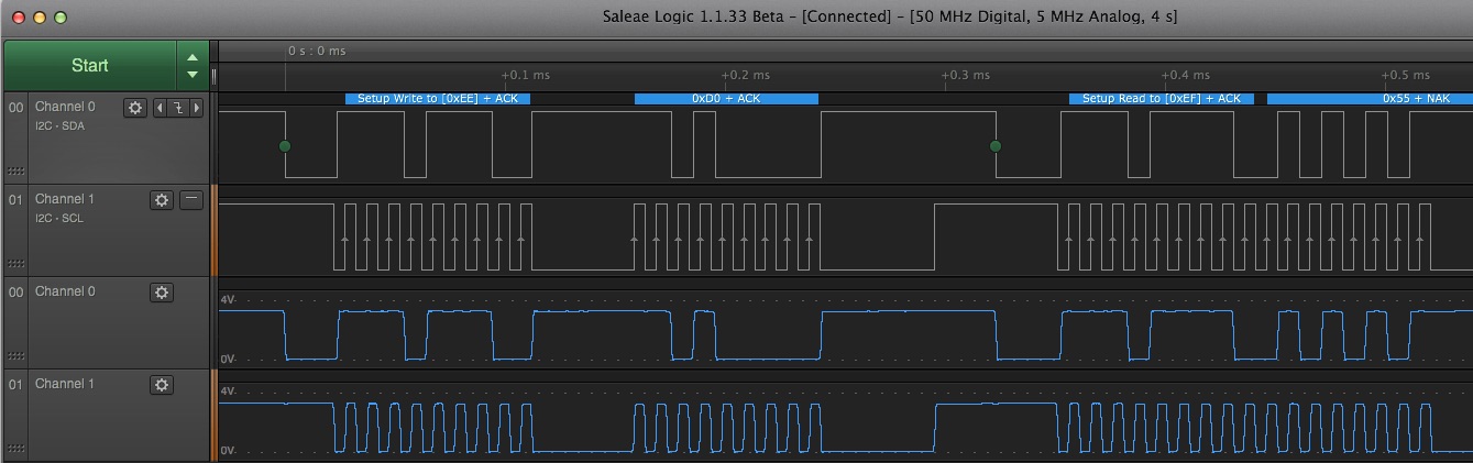
It has to look this way. The sequence just reads the static device ID for test purposes.
Outlook
In future versions, a small capacitor at the Allegro signal pin can serve as a hardware low pass filter (thanks to Ingo on the rc-heli.de forum). Additional cell voltage measurements would be nice as well.
Share